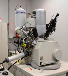
Focused Ion Beam (FIB)
 FIB consists of a high-resolution SEM column with a fine-probe Ga ion source. The
Nova Nanolab FIB has high-resolution electron (~1.5 nm) and ion (~5 nm) columns.
Its electron column is equipped with a field emission gun that is capable of the accelerating voltages ranging from 30kV to as low as 500V with an innovative "Through the Lens" detector technology. OmniProbe AutoProbe 200 in-situ sample lift-out system allows the preparation of site-specific TEM samples without the need for support films.
The FIB has an integrated HKL EBSD package to allow for orientation imaging. Light element EDS X-ray detector allows for elemental analysis, including elemental mapping. The FIB is also equipped with a Nanomechanics InSEM mechanical properties microprobe. The InSEM features a precision nanomechanical actuator, which provides highly resolved force and displacement measurements. Typical applications include TEM sample preparation from specific areas of bulk or thin film samples, site-specific cross-sectional analysis for microelectronics devices and nano-machining and nano-deposition of conductors or insulators.
- Nova Nanolab 600 from FEI
- Electron and ion guns with Schottky field emitters
- This FIB/SEM is equipped with
- TEM sectioning + manual TEM sample lift-out system
- Oxford INCA EDS for elemental analysis and mapping
- HKL EBSD for crystal orientation measurement and mapping
- 3D imaging and structural/chemical analysis capability
- Advanced control of gases for deposition, etching and milling
- High resolution patterning engine
Instrument Manager: Steve Cain
Backup: Jennifer Sammakia