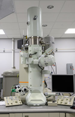
Transmission Electron Microscope (TEM)

In TEM, high energy electrons (typically from 80 to 300 keV) go through the samples with <100nm thickness to generate various signals that can be used for imaging, electron diffraction and elemental analysis. TEM is particularly useful for: high resolution imaging using bright-field (BF) and dark-field (DF) techniques and chemical analysis using energy dispersive X-ray spectroscopy (EDS) and electron energy loss spectroscopy (EELS).
The analysis performed with very high spatial resolution, typically from a few micrometers down to a couple of nanometer scales in inorganic and organic samples. Its application includes: Nano-sized structure imaging with its chemical composition analysis; micro and crystal structure analyses such as lattice defect and domain structures; crystal growth mechanism study for epitaxially grown thin film materials; and in situ observation of thermally induced structural and chemical transformation in inorganic materials using heating and cooling holders.
- High resolution TEM, JEOL JEM 2100F
- Ultra high resolution: Point to point: 0.19 nm
- Atomic lattice image: ~0.15 nm
- Minimum probe size: ~0.5 nm
- This TEM is equipped with
- Ultra high resolution STEM detectors (BF, DF and HAADF) with 0.20 nm resolution
- Compositional and chemical analysis capabilities with EDS, EFTEM, and EELS detectors
- Dual acceleration voltages: 200 kV for inorganic materials, 120 kV for biological materials
- Field-free Lorentz Imaging
- Full Remote Operation
- Dry Pumping System
- Optical Bench - Free Lens Control
- In situ heating (< ~1000oC) and cooling (liquid nitrogen) holders
Instrument Manager: In Tae Bae
Backup: Jenny Amey