New way to cool computer chips involves laser metal printing
The design will save energy and reduce toxic electronic waste – welcome news for data centers, gamers and anyone with high-end electronics.
Researchers from Binghamton University’s Mechanical Engineering Department have developed a manufacturing technique that will keep electronics cooler by 10 degrees Celsius (18 degrees Fahrenheit), allowing for faster, more efficient computation.
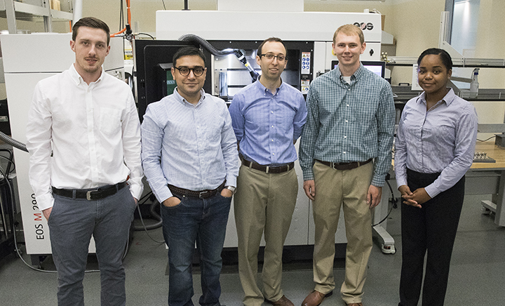
Assistant Professor Scott Schiffres and graduate students Arad Azizi and Matthias A. Daeumer who worked on the study explained that those 10 degrees are vital when it comes to saving power and reducing toxic electronic waste.
“Lower operating temperatures will improve the energy efficiency of data centers by about five percent, which can save $438 million dollars in electricity and can prevent 3.7 billion pounds of carbon dioxide from being emitted per year,” Schiffres said. “It will also reduce toxic electronic waste by about 10 million metric tons – enough to fill 25 Empire State Buildings – because of the lower rates of heat-based device failure.”
“It will mean big changes for high-end electronics, data centers and computationally intense programs such as video editing tools and video games.”
Traditionally, electronics are cooled using a heat sink that transfers the heat generated by the electronic system into the air or a liquid coolant. For instance, the central processing unit (CPU) or the graphics processors inside laptops are cooled by a heat sink.
For the heat sink to work, it has to be attached to the CPU or the graphics processor via a thermal interface material, such as thermal paste. It helps facilitate the transfer of heat by bridging microscopic gaps between the heat sink and the chip. With conventional processors, the first layer of the thermal interface material attaches the processor to the lid and a second thermal interface material attaches the lid to the heat sink. Even though the thermal interface material cools better than leaving air gaps between the heat sink and the chip, that thermal interface material impedes heat flow and leads to higher chip temperatures.
Schiffres and his team developed a way to completely remove thermal interface materials. They used a laser to selectively melt and bond an alloy directly onto the silicon of the CPUs or graphics processors.
“We plan to print microchannels on the chip itself to make spirals or mazes that the coolant can travel through directly on the chip instead of using the thermal paste as the connection between the heat sink and the chip,” explained Schiffres. “We tested the technique in Binghamton’s Electronics Reliability Lab and cycled them continuously from 130 degrees Celsius to -40 degrees Celsius for a week to make sure they could withstand constant, heavy use. All parts passed without noticeable failure or defects.”
Printing the microchannels onto the chip was not a straightforward task. Most metals and alloys will not form a good bond with the silicon due to poor adhesion with silicon and thermal expansion mismatch.
The researchers used a tin-silver-titanium alloy that will rapidly form a thin bonding layer – about 1,000 times thinner than the diameter of a human hair – in the form of a titanium-silicide that acts as a glue between the silicon chip and the metal alloy. This alloy solidifies at a low temperature, which leads to lower thermal stress from thermal contraction during cooling. By laser processing, the time to create this silicide bond was reduced to microseconds, which is sufficiently fast to allow additive manufacturing of metal directly onto silicon.
This solution removes both the lid and two thermal interface materials by printing the heat sink directly onto the silicon, giving heat a shortcut and lowering chip temperatures.
Schiffres was inspired by hardcore computer gamers who often void their own computer warranty by removing the factory installed lid and the first layer of thermal interface material to place the heat sink closer to the chip – a procedure known as de-lidding.
The study titled “Additive Laser Metal Deposition onto Silicon” will be published in an upcoming issue of Additive Manufacturing and became available online Sept. 24, 2018.
The SUNY Research Foundation is investing in patenting this advance for using laser and other rapid bonding techniques to manufacture heat removal devices on semiconductors. Schiffres team members are exploring customer demand for initial and potential use cases through the National Science Foundation (NSF) I-Corps training delivered by the Binghamton University Office of Entrepreneurship and Innovation Partnerships.

